1成果简介
石墨烯非凡特性的开发取决于能否找到在不破坏其基本结构的前提下进行合成与加工的新方法。本文,澳大利亚卧龙岗大学Gordon G. Wallace、David L. Officer等研究人员在《Small》期刊发表名为“Additive-Free Edge-Functionalized Graphene Dough”的论文,研究通过选择性氧化与物理剥离的结合,实现了直接从石墨合成高加工性、高分散性边缘功能化石墨烯(EFG)。显微镜与光谱表征揭示出该材料具有无缺陷基底层的少层石墨烯纳米片,其边缘呈现羧酸盐与酚醛基团功能化。
其无缺陷特性体现在高达900 S cm?1的导电性上。该EFG在水溶剂与有机溶剂中均展现出优异的分散性(100 mg mL?1),可形成柔性石墨烯面团并塑造成任意几何形状。干燥后的面团可迅速重新吸收多种溶剂,表明其具有高度多孔性和两亲性。通过构建3D打印导电支架、纸质印刷电路以及制备顺磁性石墨烯面团,充分展现了该材料的独特性能。值得注意的是,通过离子液体浸渍面团可制备出悬空式与3D打印超级电容器,展现出卓越的质量比电容(210 F g?1)和高能量密度(262.5Wh Kg?1)。如此高的电容值源于电荷存储过程中高效的孔隙利用率,并得益于其独特的两亲性纳米多孔EFG结构。
2图文导读
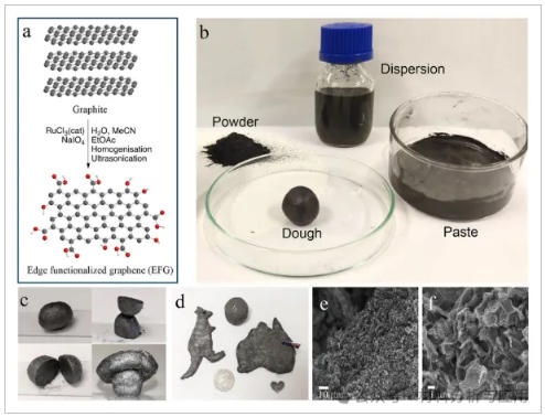
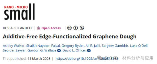
图1、(a) Schematic of the reaction of graphite to form an edge-functionalized graphene sheet. (b) Photograph showing the different forms of EFG obtained when water is added to the solid powder to give a soft dough (33 wt.% EFG), thick paste (25 wt.% EFG) and highly concentrated dispersion (100 mg mL?1 or 10 wt.% EFG). (c) Cut and molded EFG dough shapes. (d) Air-dried molded shapes of EFG dough with a 2 cm diam. coin for size comparison. (e) SEM image of the cross-section of EFG dough and (f) the magnified image showing micro/nano channels between the graphene platelets that enhance the permeation of solvents.
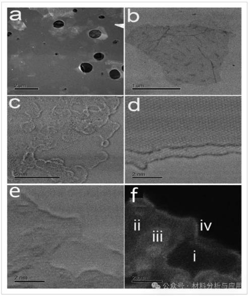
图2、TEM images of EFG at low and high magnifications. (a) Several EFG NPs are visible in the image. (b) A bright-field image of a typical EFG NP. (c) and (d) High-resolution images of the edge of a typical sheet confirming the presence of 1–4 layers. Note the edge of the EFG in c), which shows a monolayer, while in (d) 2 layers can be seen. (e) Bright field (BF) image and (f) annular dark-field image (HAADF) of a typical EFG platelet at the edge; (i), (ii) and (iii) show mono, double, and three layers, respectively, while (iv) represents an oxygen-rich area on the edge. From (i) to (iii) the diffraction is increased due to the increase in the number of layers, while at the edge (iv), higher diffraction is as a result of the presence of heavier atoms, presumably two oxygen atoms on top of each other to form a COOH group.
图3、Raman spectra of EFG at (a) nanoplatelet centre and (b) edges obtained using 632 nm laser excitation. (c) XRD spectrum of EFG. (d) Comparison of XRD peaks of graphite and EFG. Deconvoluted XPS spectra of EFG for e) C1s and f) O1s.
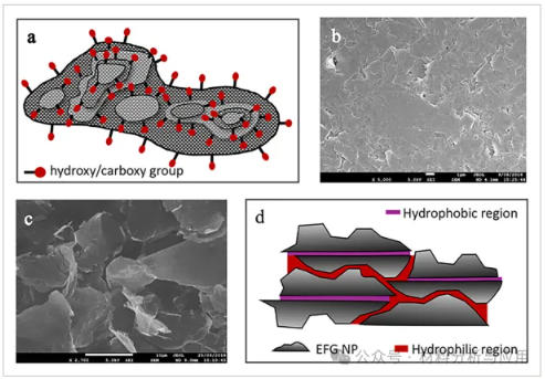
图3、(a) Schematic of the proposed structure of an EFG NP. (b) Surface view of EFG paper at low magnification and (c) high magnification. (d) Representation of interacting EFG NPs in an EFG dough containing hydrophobic (purple) and hydrophilic (red) channels.
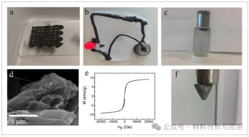
图4. (a) Photo of a 3D printed EFG scaffold. (b) Photo of a circuit extruded on paper with xanthan gum:EFG dough, lighting an LED using a coin cell. (c) Photo of Fe-EFG powder attracted to a magnet. (d) SEM image of thermally annealed EFG/FeCl3 mixture (Fe-EFG). (e) Magnetic hysteresis loop of Fe-EFG dough. (f) Photo of moldable Fe-EFG dough attracted to a magnet.
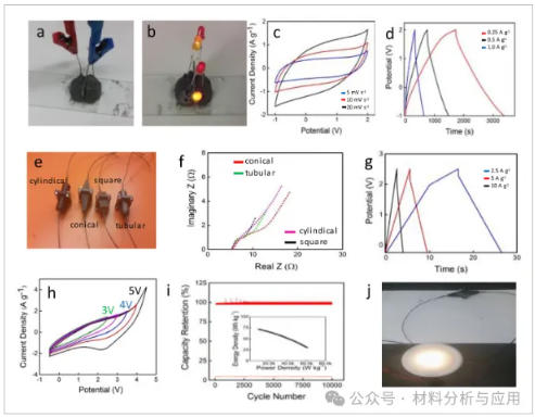
图6、Photos of a free-standing EFG dough supercapacitor (a) while being charged and (b) powering four LEDs. (c) CVs of EFG in C4mpyrFSI electrolyte in a two-electrode coin cell supercapacitor at scan rates of 5, 10 and 20 mV s?1. (d) Galvanostatic charge–discharge curves of the two-electrode coin cell supercapacitor containing EFG in C4mpyrFSI electrolyte at current densities of 0.25, 0.5 and 1 A g s?1 at a potential difference of 3 V. (e) Photos of 3D printed EFG supercapacitors. (f) Nyquist plots of the four different 3D printed EFG supercapacitors. (g) Galvanostatic charge–discharge curves of the square 3D printed supercapacitor at current densities of 0.25, 0.5 and 1 A g s?1 at a total potential difference of 3 V. (h) CVs of EFG in C4mpyrFSI electrolyte in the square 3D printed supercapacitor at a scan rate of 100 mV s?1 at different total potential ranges of 3, 3.5, 4, 4.5 and 5 V. (i) Cycling stability of the square 3D printed EFG supercapacitor over 10 000 cycles at a current density of 5 A g?1 (inset: Ragone plot of energy density versus power density). (j) Photo of the conical 3D printed EFG supercapacitor powering a LED light of 30 lumens brightness.
3小结
综上所述,通过采用含氧化钌(RuO?)的成熟催化氧化工艺,结合快速均质化和超声处理,成功从石墨直接合成了具有极 低缺陷率、卓越溶剂亲和力及分散性的边缘功能化石墨烯(EFG)。与典型单层石墨烯在水中的分散度低于5 mg mL?1不同,EFG在水溶剂和有机溶剂中均展现出高达100 mg mL?1的优异分散性。令人意外的是,仅需手工混合60%–65%的水或溶剂,即可形成柔软的石墨烯糊状物,当溶剂浓度达75%时则形成可塑性极强的膏状物。这种水基EFG糊料可塑造成任意三维或几何形状,经干燥后可重新浸渍多种溶剂。
显微镜与光谱表征揭示,EFG本质上是无缺陷的少层石墨烯,其边缘经羧酸盐和酚醛基团功能化处理,造就了非凡的分散性和两亲性。疏水性溶剂被水性糊状物吸收的现象表明,糊状物中同时存在亲水通道与疏水通道:少层纳米片层间相互作用形成的基底平面构筑疏水通道,而片层间边缘官能团的相互作用则形成亲水通道。纳米片基底层的无缺陷特性赋予面团高导电性,使EFG纸张展现出900 S cm?1的卓越导电性能。
EFG面团的纳米孔隙结构与高导电性,为验证这种独特石墨烯的应用潜力提供了契机。通过3D打印柔性EFG面团形成水溶性导电支架,而向EFG中添加黄原胶则实现了在纸张上挤出印刷防水电路。通过在EFG纳米片上形成并烧结铁酚类复合物,成功制备了氧化铁功能化顺磁石墨烯面团。
通过制备离子液体浸渍面团,成功制造出功能性自由悬浮电双层电容器(EDLC)。在硬币电池中,无粘合剂的离子液体EFG面团电极展现出卓越的质量比电容(210 F g?1),并伴随高比表面积电容(280 mF cm?2)。其能量密度达262.5 Wh Kg?1,超越多数已报道的石墨烯超级电容器。如此高的电容值表明电荷存储过程中实现了高效孔隙利用率,印证了EFG独特的两亲性纳米多孔结构。为验证EFG糊料制备可变形EDLC的潜力,通过3D打印技术制备了不同形状的EDLC并进行对比。实验表明其电化学特性与电容值高度一致,且表现出卓越的稳定性——经10,000次循环测试后仍保持95%的库仑效率。其中3D打印EFG面团电容器的能量密度(71.7 Wh kg?1,功率密度10 kW kg?1)达到商用电容器的三倍。
实现石墨烯在广泛应用中的潜力面临的主要挑战之一,在于寻找针对不同应用场景的加工方法。本文所述的EFG技术开辟了全新路径,可将石墨烯以粉末、分散液、浆料及糊状物形式,通过水溶液、有机溶剂及离子液体进行加工——这些加工方式此前均无法实现。特别是这种独特的纳米多孔两亲性EFG糊料,为复合材料开发、医疗应用支架的3D打印、新型导磁材料、无粘结剂可变结构储能电极及其他前所未有的石墨烯相关应用提供了全新机遇。
文献: