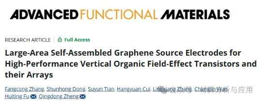
图1、a) Schematic of the self-assembly and transfer protocol for the graphene electrodes at the air-liquid interface. b) Raman G-band intensity mapping (30 µm × 30 µm) assessing the graphene uniformity across various graphene dispersion concentrations (0.01–1.00 wt.%). c) Representative SEM image of the SGS electrode. d) AFM topography image of the SGS electrode (RMS roughness: 0.87 nm). e) UPS analysis the SGS electrode. f) Raman spectrum showing characteristic graphene bands.
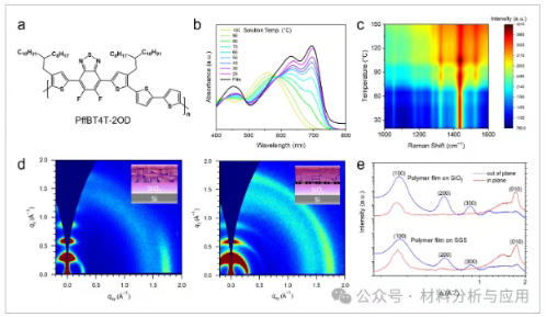
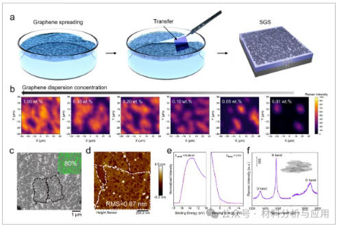
图2、a) Molecular structure of PffBT4T-2OD. b) Absorption spectra of PffBT4T-2OD film and solution (0.05 mg mL?1 in CB) with varying temperatures. c) In situ Raman monitoring of film states (λex = 473 nm). d) 2D GIWAXS patterns of PffBT4T-2OD films on bare SiO2 (left) and on SGS (right). e) In-plane and out-of-plane line-cuts for the PffBT4T-2OD films.
图3、a) Schematic architecture of the VOFET device on the SGS electrode. b) Cross-sectional SEM image of the device (scale bar: 100 nm) with annotated layer structure. c) Subthreshold curves (ID–VGS) of VOFET based on the SGS electrode. d) Transfer curves (ID–VGS) of VOFET based on the SGS electrode. e) Output curves (ID–VDS) of VOFET based on the SGS electrode, with VGS varied from 10 to ?50 V. f) Subthreshold curve (ID–VGS) of VOFET based on the AgNWs electrode. g) Transfer curves (ID–VGS) of VOFET based on the AgNWs electrode. h) Output curves (ID–VDS) of VOFET based on the AgNWs electrode with VGS varied from 10 to ?50 V. i) Energy level alignment diagram of functional layers.
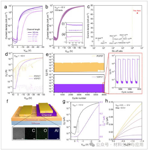
图4、a) Transfer curves for the devices with various channel lengths at VDS = ?15 V. b) Transfer characteristics of a single VOFET during 100 consecutive I?V sweeps, with insets quantifying i) current density retention and ii) threshold voltage drift. c) The maximum Ion/Ioff and current density values of the polymeric VOFETs reported in this work and in the literature. d) Transfer curves of POFET and VOFET. e) The 6000 cycle switching tests of POFET and VOFET (test frequency?=?1?Hz, VDS = ?15 V, VGS = ?50 and 0 V, alternately). f) Schematic architecture of the low-voltage VOFET based on aluminum oxide (scale bar: 5 µm). g) Transfer curves (ID–VGS) of the low-voltage VOFET based on aluminum oxide. h) Output curves of the low-voltage VOFET based on aluminum oxide.
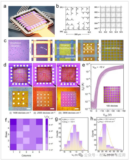
图5、a) Schematic architecture of the monolithically integrated VOFET array. b) Circuit design diagram for the VOFET array. c) Integrated process flow. d) Optical images of VOFET arrays prepared at different pixel densities (scale bar: 200 µm). e) Transfer characteristic curves of 100 devices randomly selected from various 3 × 3 arrays. f) Distribution of on-off ratio for the 5 × 5 array. g) VT variation across 100 devices randomly chosen from various 5 × 5 arrays. h) Current density statistics of 100 devices randomly chosen from various 5 × 5 arrays.