1成果简介
可集成的高性能三维微型超级电容器(MSCs)的开发为微型化储能技术带来希望,但需要先进的器件架构和可靠紧凑的制造平台。本文,广东以色列理工学院Woo Jin Hyun副教授《ACS Appl. Energy Mater》期刊发表名为“3D Aerosol-Jet-Printable Graphene Microsupercapacitor Arrays with Hollow Pillar Electrodes for High Voltage and Integration Density”的论文,研究提出采用气溶胶喷射可打印的中空柱状电极(HPEs)构建三维石墨烯超级电容器,实现高集成密度的高压阵列。
通过采用聚丙烯碳酸酯作为稳定剂配制石墨烯墨水,增强了3D打印的结构完整性;气溶胶喷射技术则可精确制备形态均匀、高度可调的垂直排列中空柱状电极。相较于传统梳状电极,中空柱状电极能形成更均匀的电场分布并增大有效表面积,从而显著提升MSC的单位面积电容。该高密度电极器件还展现出卓越的弯曲稳定性,其独特微结构可降低变形过程中的机械应力。通过串联10个高密度电极器件(单器件占地仅0.0098平方厘米),成功演示了10伏微型储能阵列,实现超高器件密度(102 cm–2)与面积电压输出(102 V cm–2)。这些成果凸显了气溶胶喷射可打印HPE技术在实现超紧凑、机械强韧且高压的储能集成领域的巨大潜力。
2图文导读
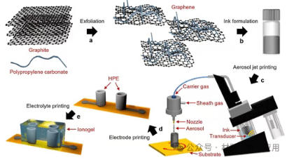
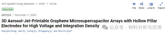
图1. Schematic diagram illustrating the AJP process of 3D graphene MSCs with HPEs. (a) Exfoliation of graphene using PPC as a stabilizer. (b) Ink formulation with the exfoliated graphene and PPC. (c) Ink setup for 3D AJP of the graphene ink. (d) AJP of 3D graphene HPEs. (e) AJP of an ionogel electrolyte on the printed electrodes to complete the MSC fabrication.
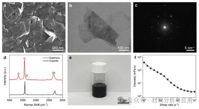
图2. Exfoliated graphene and its ink. (a) SEM image of exfoliated graphene nanoflakes. (b) TEM image and (c) selected area electron diffraction pattern of the graphene nanoflakes. (d) Raman spectra of the exfoliated graphene and graphite, highlighting characteristic D, G, D′, and 2D bands. (e) Photograph of a graphene ink formulated using the exfoliated graphene nanoflakes and PPC. (f) Viscosity of the graphene ink with a graphene-to-PPC ratio of 5:5 as a function of shear rate at 20 °C.
图3. Printed graphene HPEs. (a) Top-view and (b) side-view SEM images of an HPE prepared by AJP. (c) Thickness of HPEs printed with different numbers of printing passes. (d) Top-view and (e) side-view optical microscopy images of HPEs printed on a polyimide substrate for an MSC. (f) Photograph of the HPEs placed on a fingertip.
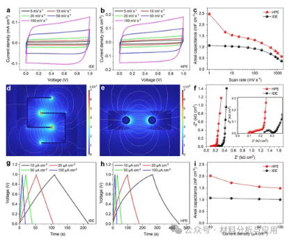
图4. Electrochemical performance of single devices. CV profiles of MSCs with (a) IDEs and (b) HPEs at scan rates from 5 to 100 mV s–1. The IDEs and HPEs were printed with the same thickness of 220 μm. (c) Areal capacitance of the MSCs as a function of scan rate from the CV measurements. Horizontal cross-sectional views of electric field distributions in COMSOL simulations for MSCs using (d) IDEs and (e) HPEs. (f) Nyquist plots of the devices with the inset showing an enlarged view of the high- and mid-frequency regions. GCD curves of the MSCs with (g) IDEs and (h) HPEs at current densities from 10 to 100 μA cm–2. (i) Areal capacitance of the devices as a function of current density from the GCD measurements.
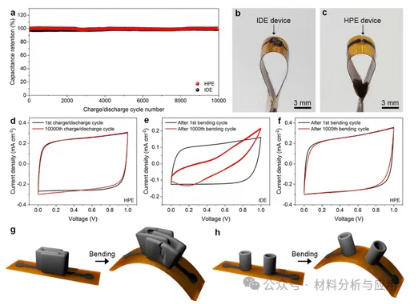
图5. Cycling and bending stability. (a) Capacitance retention of MSCs with IDEs and HPEs for 10,000 charge/discharge cycles. Photographs of MSCs using (b) IDEs and (c) HPEs on bent substrates with a bending radius of 2.5 mm. (d) CV profiles of the HPE device for the first and 10,000th charge/discharge cycles. CV profiles of the devices with (e) IDEs and (f) HPEs before and after 1000 bending cycles. All CV profiles were acquired at a scan rate of 100 mV s–1 in the flat state of the devices after the bending cycles. Schematic illustrations of (g) HPEs and (h) IDEs before and after bending.
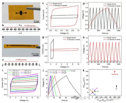
图6. MSC integration. (a) Photograph and (b) schematic circuit diagram of an array of 10 HPE devices connected in parallel. (c) CV profiles of the parallel-connected array and a single HPE device at a scan rate of 100 mV s–1. (d) GCD curves of the parallel-connected array and the single device at a current of 0.1 μA. (e) Photograph and (f) schematic circuit diagram of an array of 10 HPE devices connected in series. (g) CV profiles of the series-connected array and a single HPE device at a scan rate of 100 mV s–1. (h) GCD curves of the series-connected array and the single device at a current of 0.1 μA. (i) CV profiles of the series-connected array at scan rates from 100 to 500 mV s–1. (j) GCD curves of the series-connected array at currents from 0.1 to 0.5 μA. (k) Comparison to the integration density (1/Ssingle) and areal voltage output (Voutput/Ssingle) of previously reported 3D-printed MSC arrays in series connections for high-voltage operation, where Ssingle and Voutput denote the footprint of a single device and the output voltage per device, respectively.
3小结
本文,展示了采用气溶胶喷射可打印石墨烯高密度聚合物薄膜(HPEs)制备的高集成度高压3D微型储能器阵列。由溶液剥离石墨烯纳米片与PPC稳定剂组成的石墨烯墨水,支持纳米片在3D气溶胶喷射工艺中实现可靠的垂直堆叠,从而制备出高度可控的精细化高电极厚度结构。相较于传统电极设计,该结构能产生更均匀的电场分布,并在相同电极厚度下增大有效表面积,从而提升3D微电极阵列的面积电容。该HPE结构还能缓解弯曲时的机械应力,显著提升3D MSCs的机械柔韧性。最终实现了由10个HPE器件组成的10V阵列,单器件占地仅0.0098 cm²,达成102 cm?²的高器件密度及102 V cm?²的面积电压输出。总体而言,本研究为高性能3D微型超级电容器确立了极具前景的印刷策略与器件架构,推动了高电压与高集成密度芯片级电源的发展。虽然本研究采用石墨烯材料进行验证,但该印刷策略与器件架构有望推广至其他纳米材料制备3D微型超级电容器。
文献: